Open Compiler Explorer, paste four lines of standard C++ concurrency primitives, and compile them for both x86-64 and AArch64 with optimization flag -O3:
#include <atomic>

std::atomic<int> g_x{0};

void sync_operations() {
    g_x.store(1, std::memory_order_release);
    int val = g_x.load(std::memory_order_acquire);
    g_x.fetch_add(1, std::memory_order_relaxed);
    std::atomic_thread_fence(std::memory_order_seq_cst);
}
The resulting assembly reveals the divide immediately:
# --- x86-64 (GCC 14.2) ---
sync_operations():
    mov     DWORD PTR g_x[rip], 1       # release store: standard mov!
    mov     eax, DWORD PTR g_x[rip]     # acquire load: standard mov!
    lock xadd DWORD PTR g_x[rip], eax   # atomic RMW requires LOCK prefix
    lock add QWORD PTR [rsp], 0         # seq_cst fence: locked stack no-op!
    ret

# --- AArch64 (GCC 14.2) ---
sync_operations():
    adrp    x0, g_x
    mov     w1, 1
    stlr    w1, [x0, :lo12:g_x]         # release store: specialized STLR
    ldar    w2, [x0, :lo12:g_x]         # acquire load: specialized LDAR
    mov     w1, 1
    ldadd   w1, w2, [x0, :lo12:g_x]     # LSE atomic add: in-silicon RMW
    dmb     ish                         # seq_cst fence: inner-shareable barrier
    ret
On x86, release and acquire operations look free: they compile down to standard mov instructions. On ARM64, the programmer must explicitly emit specialized stlr and ldar opcodes. But when you ask for a sequential consistency fence, the situation flips: ARM emits an explicit data memory barrier (dmb ish), while x86 serializes the memory controller via an expensive locked store-buffer drain (lock add QWORD PTR [rsp], 0 or mfence).
The two processors arrive at the same destination, but they make opposite promises to the programmer.
The Core Takeaway: The classic textbook war between RISC and CISC ended decades ago when both sides converged on out-of-order execution engines running internal micro-operations. In 2026, the instruction set architecture (ISA) no longer dictates execution throughput. Instead, the ISA survives in three specific places where it still bills you:
- As an immutable software contract: Memory consistency defaults (x86 TSO vs ARM weak ordering), register counts, and ABI calling conventions that compilers cannot paper over.
- As a hardware budget trade-off: Silicon die area spent on decoded micro-op caches (x86) versus massive L1 instruction caches (Apple Silicon).
- As an instrument of legal sovereignty: Proprietary licensing litigation (Arm vs Qualcomm) versus royalty-free specification profiles (RISC-V RVA23).
1. The Categories Died First: Silicon Convergence
The 1980s curriculum taught a binary classification: CISC processors (x86) used complex, variable-length instructions that performed memory-to-register arithmetic to maximize code density on expensive magnetic-core RAM; RISC processors (MIPS, SPARC, early ARM) used simple, fixed 4-byte instructions strictly separating computation from memory access to enable single-cycle pipelining.
In modern silicon, that textbook taxonomy is completely obsolete:
| 1980s Textbook Pillar | Modern Silicon Reality (2026) | Exemplar Implementation |
|---|---|---|
| “CISC executes complex instructions directly” | x86 decodes variable-length macro-instructions into fixed RISC-like micro-operations (micro-ops) before execution. | Intel Lion Cove, AMD Zen 5 decode into an internal superscalar RISC core. |
| “RISC executes one simple opcode per cycle” | Modern ARM cores fuse multiple instructions together and execute complex multi-cycle vector matrix operations. | Apple Firestorm fuses cmp + b.cc, AES pairs, and processes 128-bit LDP/STP dual-memory ops. |
| “CISC requires complex microcode ROMs” | High-performance x86 cores bypass decoders entirely using massive decoded micro-op caches. | AMD Zen 5 embeds a 6,000-entry micro-op cache feeding up to 12 instructions per cycle. |
| “RISC instruction sets are minimal and simple” | ARM64 manuals span thousands of pages covering vector extensions, pointer auth, and memory tagging. | ARMv9 introduces SVE2, SME (Streaming SVE), PAC, and MTE. |
Modern high-performance cores look virtually identical from the execution units backward. They are out-of-order, superscalar engines with hundreds of physical registers, speculative branch predictors, and multi-ported load/store queues.
The differences that survive are concentrated in the frontend and the software contract.
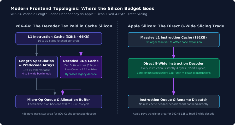
Two divergent silicon investments: x86 pays die area for a 6K-entry micro-op cache to bypass length decoding; Apple Silicon pays die area for a 192KB L1 instruction cache to feed an 8-wide direct decoder.
2. The Decoder Tax: Real, Workload-Shaped, and Already Paid For
A common claim in tech commentary asserts that x86 is permanently hobbled by a “decoder tax”: because x86 instructions range from 1 to 15 bytes in length, the CPU cannot know where instruction N+1 begins until it parses the prefixes and opcode of instruction N.
This creates a serialization bottleneck. To build a wide decoder (such as AMD Zen 5’s dual 4-wide decode clusters or Intel Lion Cove’s 8-wide decoder), x86 must run speculative pre-decode arrays to guess instruction boundaries across 16-byte fetch windows.
In contrast, ARM64 instructions are strictly fixed at 4 bytes (32 bits), naturally aligned. An 8-wide decoder (like Apple Silicon) simply slices a 32-byte cache window into eight equal 4-byte chunks with zero length speculation.
Measuring the Tax: The Zen 5 Op Cache Experiment
How much does length decoding actually cost in performance?
The clearest empirical measurement was published by Chips and Cheese, who used AMD model-specific register MSR 0xC0011021 on a Ryzen 9 9900X to physically disable the 6,000-entry micro-op cache, forcing the CPU to fetch and decode every x86 instruction from L1I through the x86 decoders:
| Workload | Op Cache Coverage (Normal) | Score Delta (Op Cache Disabled) | What the Delta Proves |
|---|---|---|---|
| SPECint (Single-Thread) | 85% to 92% | -20.3% | Large instruction footprints with high single-thread IPC hit the 4-wide decode bottleneck hard. |
| SPECfp (Single-Thread) | 78% to 88% | -16.8% | Floating point loops encounter frontend starvation when falling back to legacy decode. |
| SPECint (SMT Active) | 82% to 90% | -4.9% | Dual SMT threads interleave decode clusters, reducing decoder idle bubbles. |
| SPECfp (SMT Active) | 75% to 85% | -0.82% | Compute units become execution-bound; frontend decode speed ceases to matter. |
| Cinebench 2024 (1T) | 84.4% | -13.5% | Rendering engine loops exceed small L1I windows when op cache is bypassed. |
| Cyberpunk 2077 | 83.5% | -0.17% | Memory latency and GPU scheduling dominate; decode speed has virtually zero impact. |
| GTA V | 77.0% | 0.0% (No change) | Frame delivery is completely bound by draw calls and DRAM latency. |
The Silicon Budget Trade-Off
This benchmark data dismantles the myth that x86 is doomed by its decoders:
- The tax is already paid in silicon: Modern x86 processors hit 80% to 90% op cache coverage on typical code. The CPU spends die area on a 6,000-entry micro-op cache so that it rarely executes the legacy variable-length decoders during critical loops.
- The trade is symmetric: x86 spends transistors on decoded micro-op caches and predecode arrays. Apple Silicon spends transistors on a massive 192KB L1 instruction cache (3x larger than x86) to offset ARM64’s lower code density, and accepts one taken branch per cycle where x86 handles two.
Both approaches are rational engineering trades optimized for different markets: Apple optimized for client battery efficiency and wide low-clock throughput; Intel and AMD optimized for high-clock server density and 40 years of binary compatibility.
3. The Contract the Compiler Cannot Paper Over
While out-of-order execution engines absorb instruction encoding differences, the ISA defines a rigid contract with the compiler and the operating system.
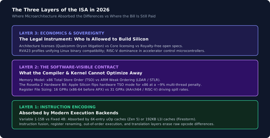
The ISA in 2026: instruction encoding is largely absorbed by execution units; the contract and economics remain immutable.
1. Memory Consistency Models: x86-TSO vs ARM Weak Ordering
The most consequential difference between architectures is the memory consistency model:
- x86 Total Store Order (TSO): Hardware guarantees that memory stores become visible in strict program order. A store cannot pass an earlier store, and a load cannot pass an earlier load. Relaxed and acquire/release memory orders compile to regular
movinstructions because the hardware enforces TSO by default. - ARM Weak Ordering: The memory bus permits aggressive reordering of loads and stores. To establish an acquire/release relationship, compilers must explicitly emit specialized instructions (
LDAR,STLR) or insert full memory barriers (DMB ISH).
x86-64 Memory Contract (Strict TSO):
Store A  =====>  Store B  (Hardware guarantees visibility order: B never seen before A)

ARM64 Memory Contract (Weakly Ordered):
Store A  ---\ /---  Store B  (Reordered by interconnect unless guarded by STLR or DMB)
             X
Store B  ---/ \---  Store A
The Rosetta 2 Hardware Trick
When Apple built the M1 chip to run x86 binaries via Rosetta 2 translation, they encountered a severe architectural challenge: emulating x86 TSO semantics on a weakly-ordered ARM64 core requires injecting memory barrier instructions (DMB) around almost every translated memory access. Doing so in software degrades translation performance by 30% to 40%.
Apple’s solution was pure engineering audacity: they added an undocumented hardware register bit to their CPU cores.
When the macOS kernel schedules an x86 binary running under Rosetta 2, it flips an internal CPU control register:
ACTLR_EL1.TSO = 1
This hardware switch puts the Apple Silicon core into x86 Total Store Order mode. The memory controller’s store queue begins enforcing x86 store ordering rules directly in silicon.
The cost? Benchmarks measuring Apple Silicon with hardware TSO enabled show a ~9% performance penalty on multi-threaded SPEC workloads due to conservative store-buffer draining. But that 9% silicon tax was vastly cheaper than the 40% penalty of software barrier emulation.
This is the ultimate proof that the ISA matters: an entire physical hardware mode exists in Apple Silicon solely to honor another architecture’s memory contract.
The Sunset of Rosetta 2
Apple published a developer update confirming that general-purpose Rosetta 2 support will sunset after macOS 27, leaving only a narrow compatibility layer for legacy games. The bridge was built to migrate the ecosystem; once the software contract migrated natively to AArch64, the hardware justification for maintaining x86 TSO modes disappeared.
2. Register Pressure and Code Density
- General Purpose Registers: Classic x86-64 exposes only 16 architectural GPRs. ARM64 and RISC-V expose 31 and 32 GPRs respectively. In tight mathematical loops, 16 registers force the compiler to spill variables to the stack cache, increasing load/store instruction traffic. Intel’s APX (Advanced Performance Extensions) finally expands x86 to 32 GPRs with 3-operand instruction syntax, acknowledging the register-pressure penalty.
- Code Size & Instruction Cache Footprint: Because x86 instructions are variable-length (1 to 15 bytes), CISC code is dense. A single x86 instruction can encode complex scaled addressing and arithmetic:
ADD [rax + rbx*4 + 0x20], edxOn ARM64, the same operation requires separate address calculation, load, add, and store instructions. Consequently, ARM64.textsections are commonly 10% to 25% larger than equivalent x86-64 binaries, requiring larger L1 instruction caches to maintain parity.
4. The ISA as a Legal and Economic Instrument
Beyond silicon and compilers, the modern ISA operates as a legal instrument dictating who is allowed to manufacture microprocessors.
1. The Three Licensing Models
- The x86 Closed Duopoly: Intel and AMD maintain a perpetual cross-licensing patent treaty. No third party can license x86 to build custom server or mobile silicon. If a cloud hyperscaler wants custom silicon, x86 is legally unavailable.
- The ARM IP Licensing Model: Arm Ltd licenses both pre-designed CPU cores (Cortex-X, Neoverse) and Architectural Licenses (allowing companies like Apple and Qualcomm to design custom microarchitectures from scratch). However, the ongoing legal dispute between Arm and Qualcomm over the Nuvia/Oryon core acquisition demonstrates the commercial friction of proprietary ISA governance.
- RISC-V Open Specification: RISC-V is an open standard governed by a Swiss entity (RISC-V International). The specification is free and cannot be revoked by export controls. Anyone can design a RISC-V core without paying royalties or requesting permission.
2. RISC-V’s Real World in 2026: The Accelerator Sub-Processor
Tech evangelists often predict that RISC-V will displace x86 and ARM in laptops and servers overnight. That view misunderstands software distribution economics.
The real challenge for application-class RISC-V is software fragmentation. Because RISC-V was designed as a modular base with dozens of optional extensions, early Linux distributions faced an explosion of incompatible binary targets. The RVA23 Profile Standard was created specifically to freeze a unified instruction baseline for commercial operating systems.
Where RISC-V is winning today is not in primary host CPUs, but inside accelerator sub-processors:
- Modern enterprise GPUs, AI accelerators, and network interface cards (SmartNICs) embed dozens of microcontroller cores to manage firmware, power domains, thermal loops, and memory telemetry.
- NVIDIA completely replaced its proprietary Falcon control microcontrollers with custom NV-RISCV32 and NV-RISCV64 cores across its GPU line.
- Western Digital and Seagate ship billions of storage controllers driven by RISC-V.
In these environments, binary compatibility with Windows or Debian is irrelevant; zero license fees and complete architectural freedom dominate.
Measuring Your Own Frontend Boundness
If you want to know whether your production workload actually cares about instruction decoding or frontend stalls, stop reading architectural debates and measure it directly with Linux perf:
# Measure topdown frontend vs backend execution metrics
perf stat --topdown -a -e cycles,instructions,frontend_retired.any_ds -- sleep 10
On Linux systems with TopDown profiling support (Intel Ice Lake / Sapphire Rapids and AMD Zen 4/5), perf splits execution cycles into four primary buckets:
[Pipeline Slots]
  ├── Frontend Bound  (Stalled on instruction fetch, decode, or uop cache miss)
  ├── Bad Speculation (Discarded work from branch mispredictions)
  ├── Backend Bound   (Stalled on memory latency, L3 cache, or execution ports)
  └── Retiring        (Useful work completed)
In 90% of real-world distributed backends (Go services, database query engines, Java runtimes), the profiler reveals that Backend Bound memory stalls account for 50% to 70% of cycles, while Frontend Bound decode stalls sit under 10%.
Unless your service is spending its life thrashing a 2MB instruction cache inside an instruction-heavy binary, the instruction set architecture is not your bottleneck. Memory bandwidth, cache hierarchy, and concurrency design dictate your latency.
Sources & Technical References
- Blem, Menon, Sankaralingam (2013): “Power Struggles: Revisiting the RISC vs. CISC Debate on Contemporary ARM and x86 Architectures” (HPCA 2013). Empirical proof that ISA differences have negligible impact on performance compared to microarchitectural implementation.
- Chips and Cheese (2024): “Disabling Zen 5’s Op Cache and Exploring its Clustered Decoder”. Primary benchmark data measuring Zen 5 performance drop with op cache disabled via MSR
0xC0011021. - Dougall Johnson (2021–2024): “Apple Silicon M1/Firestorm Microarchitecture Documentation”. Reverse-engineered measurements of 8-wide decode, coalesced retire queues, and instruction fusion.
- AMD Corporation (2024): “Software Optimization Guide for AMD Family 1Ah Processors (Zen 5)”. Architecture specs for 6K-entry op cache and dual decode clusters.
- Intel Corporation (2024): “Intel 64 and IA-32 Architectures Optimization Reference Manual”. Lion Cove 8-wide decoder and Decoded Stream Buffer (DSB) specs.
- Apple Developer Documentation (2025): “Rosetta 2 Transition & Support Lifecycle Note”. Developer schedule confirming Rosetta 2 sunset.